電気工学
System Modelerを使うと,電気回路,パワーエレクトロニクス,電気機械を構築し,研究することができます.電気と機械のコンポーネントを組み合せて完全なシステムモデルを構築したり,解析タスクを実行して性能を測定したりできます.
Flip-Flop
Flip‐flops are digital logic circuits commonly used in processes where there is a need for digital data storage and transfer. In this example we will use the Digital library, a part of the Modelica Standard Library, to demonstrate the use of basic logic gates in a pulse‐triggered master‐slave flip‐flop.
Flip‐Flop Model Structure
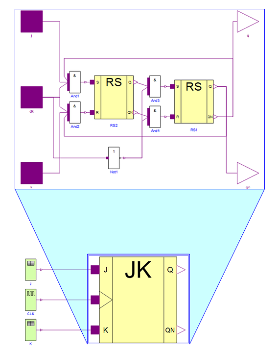
The smaller bottom image shows the flip‐flop top model as seen in the diagram view in Wolfram SystemModeler. As can be seen, the flip‐flop has three different inputs: two tables j and k containing values and a clock source CLK that provides the pulses. Going down one level into the component named JK (the expanded image at the top), we see some of the basic gates denoted And1, And2, And3, And4, and Not1. The output from these gates is calculated using the corresponding truth table.
Simulation Results
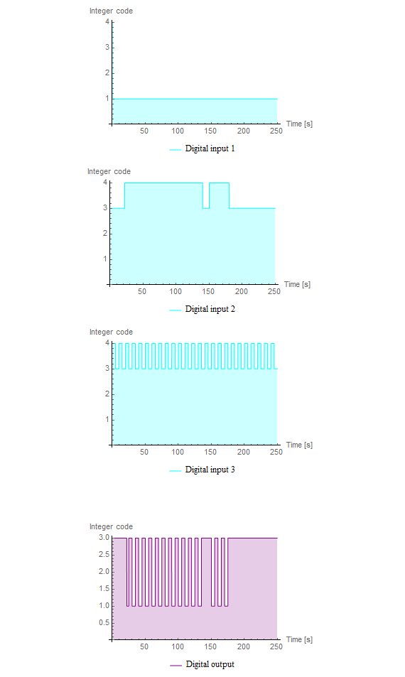
These are the simulated results of the And2 component in the flip‐flop model. This particular gate has three different inputs (shown in the top three subplots). The output, calculated from the corresponding truth table for an And basic logic gate, can be seen in the bottom subplot. In the digital library the integer codes correspond to different logic values: 1 = uninitialized, 3 = binary value 0, 4 = binary value 1.
Wolfram System Modeler
評価版
ご購入
System ModelerはWindows,macOS,
Linuxで
日本語と英語でご利用になれます »
ご質問やコメントはWolframエキスパートまでお寄せください »